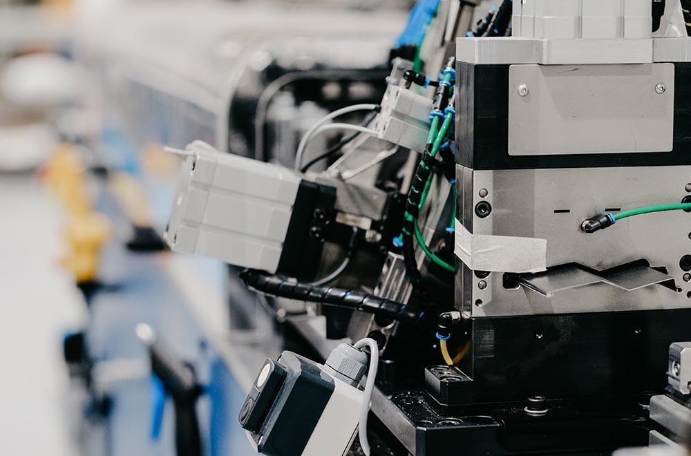
With breakthroughs in manufacturing capabilities and coupling processes, silicon photonics (SPP) technology is becoming a key driving force for the development of fiber optic modules. Compared to traditional InP architecture, SPP can integrate modulators, driver circuits, waveguides, and even parts of the DSP structure onto a single chip, achieving higher bandwidth density and lower manufacturing costs.
Industry analysts point out that SPP integration brings three major changes:
● Lower Cost Structure
Large-scale wafer fabrication processes are making optical modules more “semiconductor-like,” lowering the manufacturing threshold.
● High-Density Packaging Becomes Mainstream
More optical paths can be integrated, enabling solutions such as 4x200G and 8x100G.
● Improved Heat Dissipation
Structural optimization results in shorter heat diffusion paths and more power consumption than traditional solutions.
With improvements in the engineering capabilities of optical thin films, cavity coupling, and laser arrays, SPP has moved from “laboratory technology” to a true commercialization cycle. Several international cloud providers have begun deploying 400G modules equipped with silicon photonics engines to meet the throughput demands of large-scale AI training clusters.